We have a new session for SVC 2026!!! I am still looking for a session co-moderator and an instructor that would like to teach half or full day course on the basics of advanced semiconductor packaging and integrated photonics.
Here is the official session call:
Large Area Advanced Packaging and Integrated Photonics
The growing demand for high-performance computing, artificial intelligence, augmented/virtual reality, and advanced communication systems is driving unprecedented innovation in both large-area advanced packaging and integrated photonics. As the limits in transistor size and speed approach, the logical next steps to increase performance involve advancements in parallel computation and optimized communication between integrated components. To increase throughput, yields, thermal performance, and reduce cost, substantial focus and development effort have been put into large-area advanced packaging. As a foundational technology for these advancements, thin film deposition, a core area of expertise within the SVC community, plays a critical role in enabling the next generation of devices. This session will explore the cutting-edge intersection of large-area manufacturing techniques for advanced packaging and integrated photonics. We encourage submissions that address challenges, present novel solutions, and showcase recent advancements in manufacturing equipment, processes, materials, and architectures.
Topics of Interest Include, but are not limited to:
Large Area Advanced Packaging:
New process, equipment, performance, and yield requirements for advanced packaging,
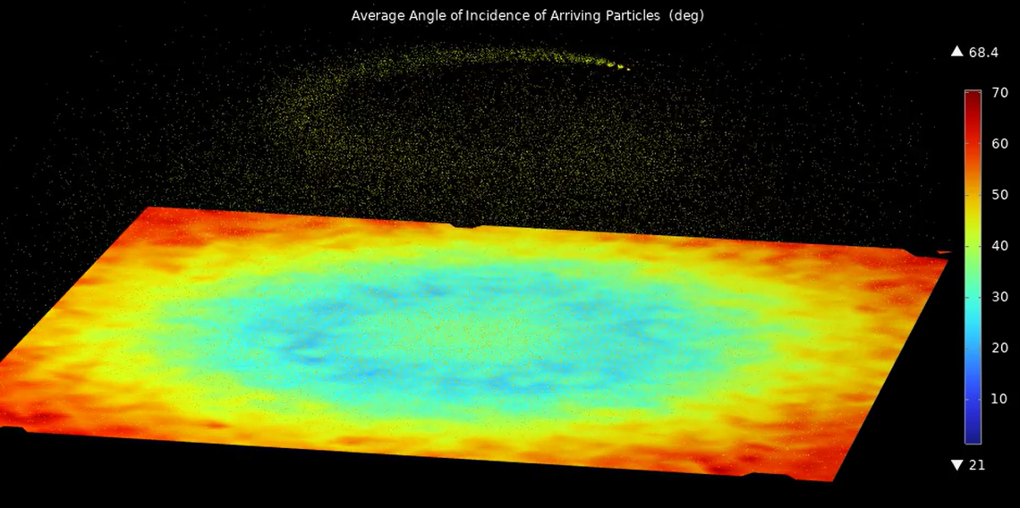
Large area packaging challenges and solutions,
Wafer-level and panel-level packaging for integrated photonics,
Advanced interconnects (e.g., through-silicon vias (TSVs) and through-glass vias (TGVs)), and
Substrate technologies and interposer solutions for large-area integration.
Thin Film Deposition for Photonic Integration:
Challenges and opportunities in scaling up integrated photonics manufacturing,
Silicon photonics and other material platforms for integrated optics,
Advanced dielectric and optical coatings for waveguides, filters, and resonators,
Deposition of active photonic materials,
The role of atomic layer deposition (ALD) and precise film control, and
Large area physical vapor deposition (PVD) techniques for metallization and optical layers.
Manufacturing and Process Control:
High-throughput manufacturing methods,
Process control and in-situ monitoring for thin film deposition, and
Yield enhancement and cost reduction strategies for large area integration.
We encourage submissions from academic and industrial researchers, engineers, and scientists working on all aspects of large area advanced packaging and integrated photonics, especially those with a focus on the underlying thin film and deposition processes.
Join us to discuss the latest breakthroughs and future directions in this rapidly evolving field.
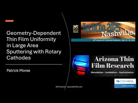
TAC Chair: Patrick Morse, Arizona Thin Film Research LLC, pmorse@azthinfilm.com